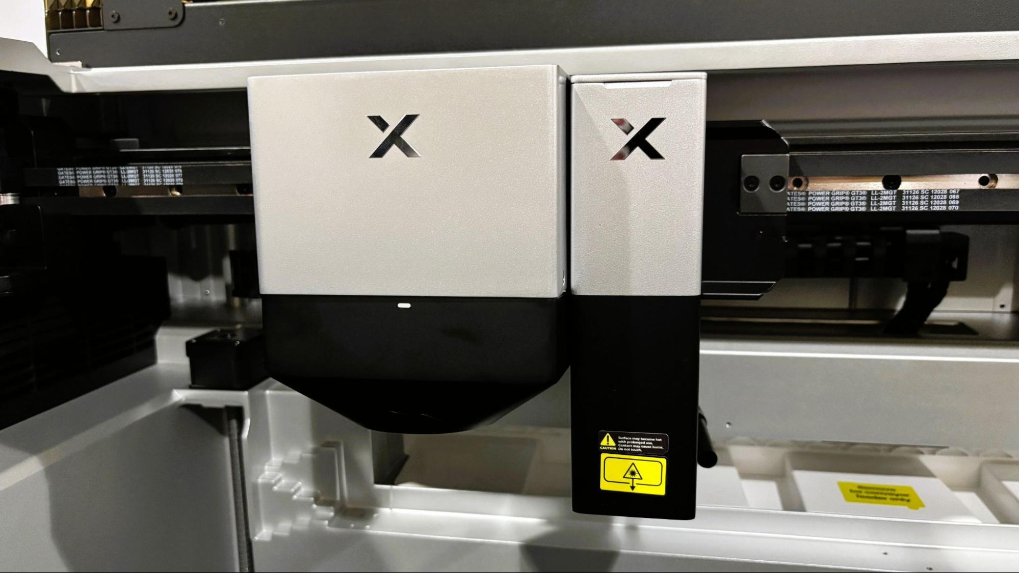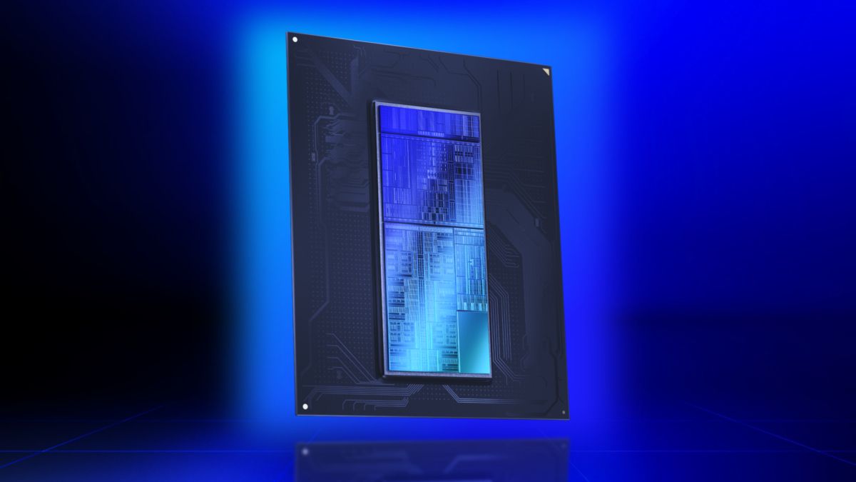
Intel has put ASML’s High NA EUV lithography into high-volume production for selected layers of its Core Ultra Series 3 processors, code-named Panther Lake, ASML said Wednesday. The claim is a useful one to parse carefully: Intel is not building the whole chip with the new scanners. It has qualified some Intel 18A layers in Oregon to run on ASML’s newer 0.55 numerical aperture tools.
ASML said this makes Intel the first company shipping high-volume logic products made with High NA EUV. The company also said those qualified layers are already moving to customers with yields comparable to wafers exposed on ASML’s existing NXE EUV platform.
The production detail that matters is dual qualification. According to ASML, the same Intel 18A layer can be exposed on either a 0.33 NA NXE scanner or a 0.55 NA EXE scanner, and the resulting wafers are interchangeable. That gives Intel Foundry more scheduling flexibility across its lithography fleet while it introduces the newer machines without betting the entire flow on them.
High NA EUV uses the same 13.5-nanometer extreme ultraviolet light as current EUV systems. The change is in the optics. ASML’s EXE platform raises the numerical aperture from 0.33 to 0.55, which lets the scanner collect and focus light more tightly on the wafer. In manufacturing terms, that can print finer features in one exposure and reduce the need for some multi-patterning steps on dense layers.
That is the reason chipmakers care. Multi-patterning adds process steps, alignment risk, time, and cost. A sharper single exposure does not magically fix advanced manufacturing, but it can improve pattern fidelity and process control on the layers that are hardest to print.
ASML President and CEO Christophe Fouquet said in the company’s announcement that High NA EUV brings “increased resolution and better process control” and supports “smaller, denser patterning” for AI and other technologies.
Intel Foundry Executive Vice President and General Manager Naga Chandrasekaran said qualifying the High NA option on selected Intel 18A product layers lets Intel use its current tool base for higher manufacturing output while preserving options for later process technologies.
The companies have been working toward this for several years. In 2024, Intel installed ASML’s TWINSCAN EXE:5000, one of the first commercial High NA EUV systems, at its Hillsboro, Oregon, research and development site. Intel later qualified ASML’s second-generation TWINSCAN EXE:5200B, which ASML describes as improving wafer throughput, overlay accuracy, and EUV source performance compared with the earlier model.
Panther Lake is already a launched client processor family, not a future tape-out. Intel introduced Core Ultra Series 3 at CES on January 5, 2026, opened preorders the next day, and put systems on shelves globally on January 27. The Core Ultra X9 378H followed in April alongside the value-tier Core Series 3, code-named Wildcat Lake. Handheld-focused Arc G3 parts arrived on May 28.
So ASML’s “shipping” language refers to wafer flow from Intel’s fab into the supply chain, rather than a new Panther Lake product launch. ASML said the companies will keep working on High NA readiness, with Intel 14A the next named process in view. Intel has designed 14A to use High NA on some of its tightest-pitch layers.
This story draws on original reporting from Tom's Hardware.