Tesla’s AI5 processor has reached tape-out at Samsung Foundry and is slated for manufacture at Samsung’s Taylor, Texas fab on the company’s latest 2nm-class process, according to James Kim, a principal engineer at Samsung Foundry.
Kim disclosed the milestone in a LinkedIn post, which was flagged by Sawyer Merritt on X. Tape-out is the point where a chip design is handed off for fabrication, so the post is a meaningful step toward production, though it is not the same thing as finished silicon shipping in volume.
Kim wrote that the “Tesla-Samsung AI5 chip” is scheduled to be built at the Taylor fab and “will soon be integrated into Tesla’s newest products.” He said Samsung engineers had worked with Tesla teams in Palo Alto and Austin over the past several months.
The Samsung tape-out follows Tesla’s earlier disclosure that AI5 would be made by both Samsung Foundry and TSMC. Elon Musk showed the first AI5 sample in mid-April and said Tesla planned to use both foundries for the processor. The TSMC implementation appears to have reached tape-out several months before the Samsung version.
What Tesla has shown so far
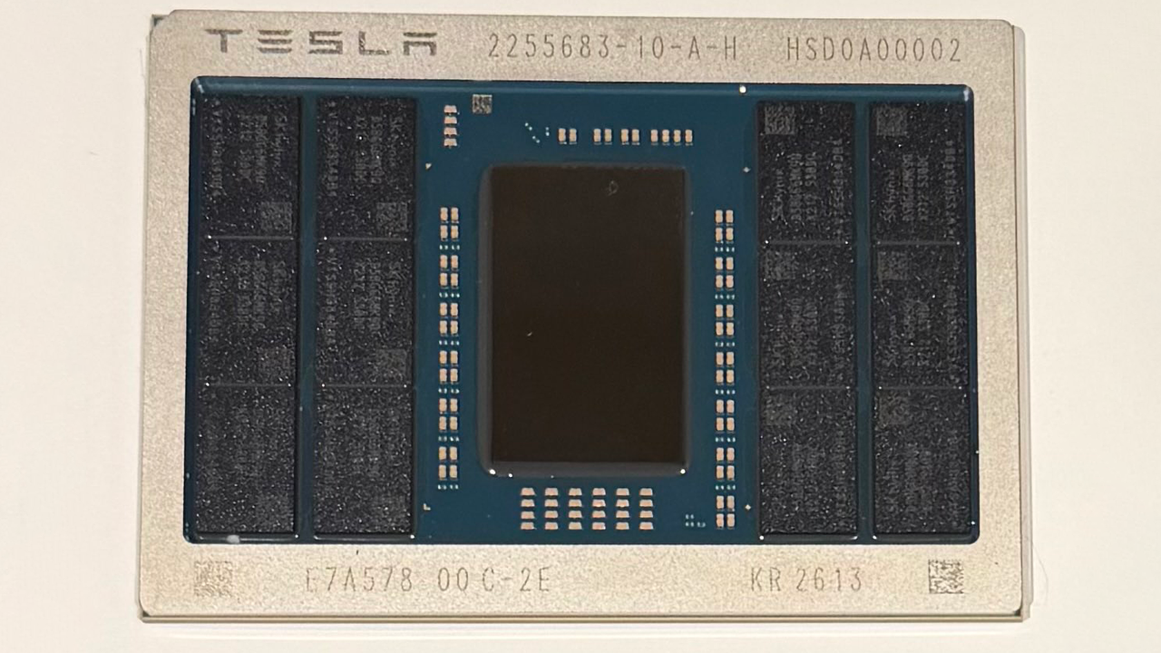
The AI5 module Musk displayed in April paired a relatively compact accelerator die with 12 SK hynix memory packages. Based on Musk’s earlier comments, the die is roughly half a reticle in size. The module uses an organic substrate, and the memory packages appear to be standard GDDR6 or GDDR7 devices rather than exotic stacked memory.
Tesla has not published the chip’s memory interface width. The visible layout, however, gives a clue: 12 GDDR6 or GDDR7 memory packages would typically imply a 384-bit external memory bus. Depending on the memory type and speed Tesla chooses, that would put bandwidth somewhere between 768 GB/s and 1.536 TB/s.
The company also has not released peak compute figures or a full specification sheet for AI5. Musk has claimed the chip can be as much as 40 times faster than its predecessor in some workloads, but Tesla has not provided public benchmark details that would let outsiders verify the comparison.
Why two foundries matter
Musk has said he expects AI5 to become one of the most-produced chips ever. That is the stated reason Tesla plans to split manufacturing between TSMC and Samsung Foundry rather than rely on a single supplier.
Tesla expects AI5 to be used across several parts of its business: vehicles, Tesla robots, and the company’s data centers. That makes the chip more than another car computer if Tesla follows through on Musk’s plan. It would become a shared silicon platform for autonomy, robotics, and AI infrastructure.
Samsung’s role is also notable because the disclosed production site is Taylor, the company’s Texas fab. Kim’s post ties Tesla’s AI5 directly to Samsung’s 2nm-class manufacturing effort in the United States, a high-profile customer win if the chip moves from tape-out into volume production on schedule.
This story draws on original reporting from Tom's Hardware.