AI photonic interconnects are becoming a front-line fight in AI hardware because the speed of a training cluster increasingly depends on how fast chips can talk, not just how many floating-point operations a GPU can claim. Nick Harris, chief executive of Lightmatter, told Tom’s Hardware Premium that processor gains can no longer come mainly from making one piece of silicon bigger, since chip size runs into physical limits.
Harris said AI systems are constrained by the need for low latency and high bandwidth between many processors. That pushes the industry toward networking dozens or hundreds of accelerators so they act more like one machine. In his words, “networking is the future of computing.”
What are AI photonic interconnects?
Photonic interconnects use light to move data between chips, boards, racks or data centers, replacing some electrical signaling over copper. In AI systems, they are being pulled closer to GPUs and switches because copper links have shorter reach, higher power costs and growing supply pressure.
The industry splits the problem into scale-up, scale-out and scale-across networking. Scale-up links accelerators inside a server, rack or pod with very low latency. Scale-out connects those systems into larger clusters. Scale-across joins whole data centers. Polina Bayvel, professor of optical communications and networks at University College London, told Tom’s Hardware Premium that hyperscalers are driven by the idea that adding more hardware improves the answer, with 72 to 144 GPUs now fitting into a single scale-up rack before the system reaches outward.
Harris said copper has already reached its practical rack-scale limit, describing usable cable reach as shorter than an arm span. That is why optics are shifting from rack-to-rack cabling toward the accelerator package itself. Elon Musk has also moved to buy Mesh Optical as part of TeraFab and SpaceX’s AI infrastructure efforts, according to Tom’s Hardware.
How optics are moving toward the processor
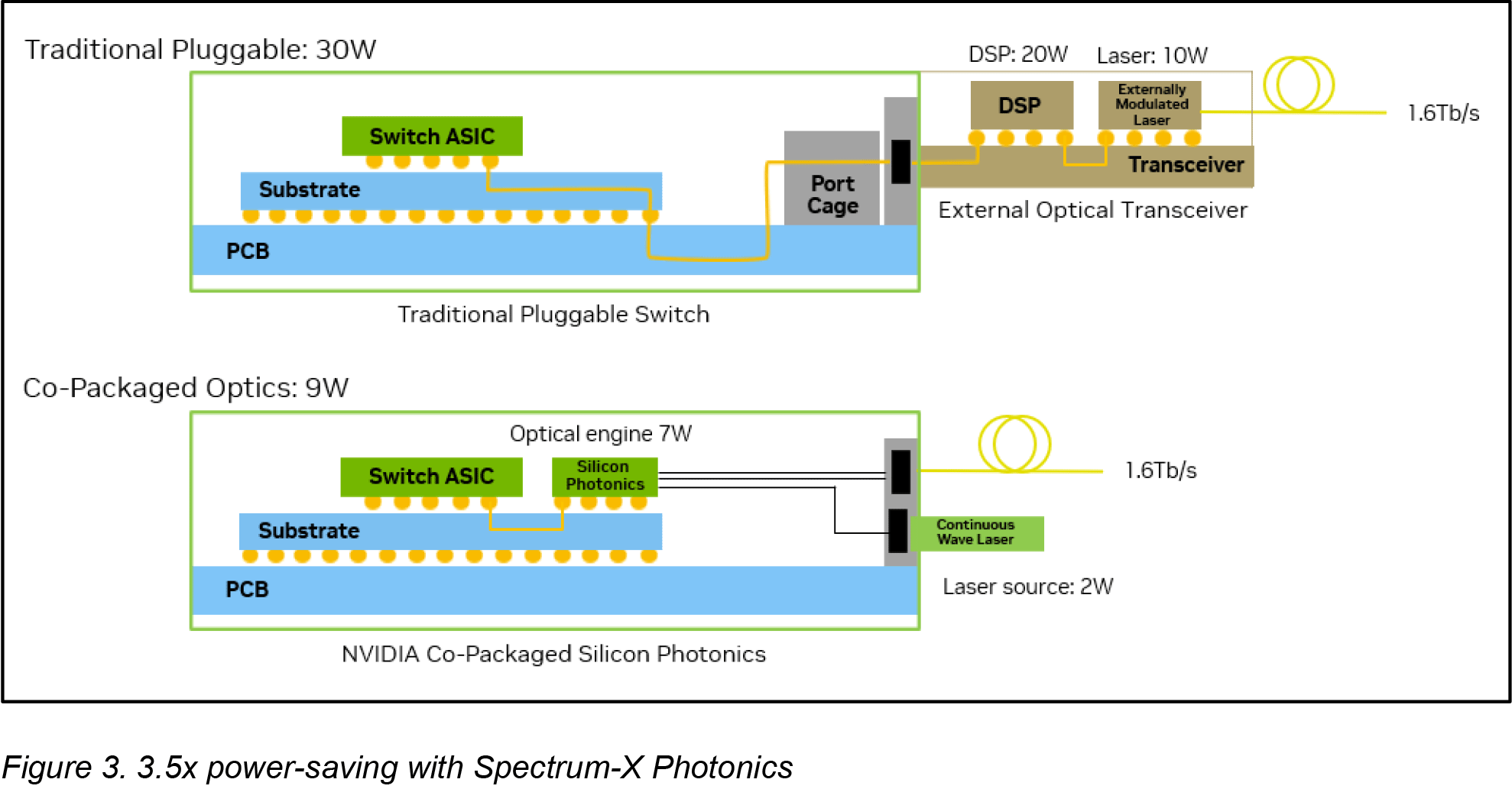
Most optical links in data centers today use pluggable transceivers placed about 18 inches from a switch. Near-package optics reduces that distance to roughly six inches. Co-packaged optics, or CPO, puts optical chiplets around a GPU or switch. A more aggressive version places optical components on an interposer below the chip.
Harris said each step should increase speed and cut energy use. He expects 2027 and 2028 to be major years for near-package optics, calling it a test bed before optical transceivers are built into accelerator or switch designs more directly. Lightmatter is building CPO parts at TSMC and GlobalFoundries and expects shipments in 2028, while also working with customers on interposer-based designs.
Power is a main reason for the shift. Bayvel said networking accounts for about 20 percent of data center energy use, with GPUs consuming the remaining 80 percent. She also warned that efficiency gains are likely to be spent on adding more GPUs rather than reducing total energy demand.
Standards and lasers are the hard parts
Nvidia has its own stack spanning NVLink and NVSwitch for scale-up, plus Spectrum-X Ethernet and InfiniBand for scale-out. Other companies, including AMD, Broadcom, Cisco, Arista, Marvell, Meta, Microsoft and OpenAI, are backing alternatives such as UALink, Ultra Ethernet and newer optical specifications.
AMD showed a 72-GPU Helios MI455X rack at Computex to compete with Nvidia’s Vera Rubin NVL72, according to Tom’s Hardware. Its scale-up fabric uses UALink-over-Ethernet rather than native UALink because dedicated UALink switch silicon from partners including Astera Labs and Marvell was not ready. Engineering samples are due in the second half of 2026, with mass production expected in Q2 2027.
Bayvel described another split between CPO and linear-drive pluggable optics. CPO may use less power but can be harder to service if a laser fails, while pluggable optics keep modules replaceable. She expects both approaches to coexist, with an estimated 60/40 lean toward CPO.
The laser supply chain is the other weak point. Frederic Gardes, professor of silicon photonics at the University of Southampton, told Tom’s Hardware Premium that silicon does not emit light, so the industry relies on III-V materials such as indium phosphide and gallium arsenide. Gardes said China controls about 80 percent of that supply, making laser integration on silicon a key problem.
In March, AMD, Broadcom, Meta, Microsoft, Nvidia and OpenAI founded the Optical Compute Interconnect Multi-Source Agreement to define a shared optical physical layer for scale-up links. The specification is intended to carry both NVLink and UALink, starting at 200Gbps per direction and scaling toward 3.2Tbps per fiber.
This story draws on original reporting from Tom's Hardware.