AMD used its Advancing AI event to detail the AMD Instinct MI455X, its next data center AI accelerator, and the Helios rack architecture that links 72 of the chips into one coherent accelerator system. That matters because Nvidia’s NVL72 rack design has set the shape of the current high-end AI server fight, and AMD is now showing a rack-scale answer rather than only a faster standalone GPU.
AMD called the MI455X the most advanced AI accelerator it has built. The company’s numbers make the pitch obvious: a very large chiplet GPU, 432GB of HBM4 memory per accelerator, and peak low-precision throughput that AMD says can exceed some figures Nvidia has disclosed for Rubin. Those are paper specs, and paper does not run inference workloads.
What is the AMD Instinct MI455X?
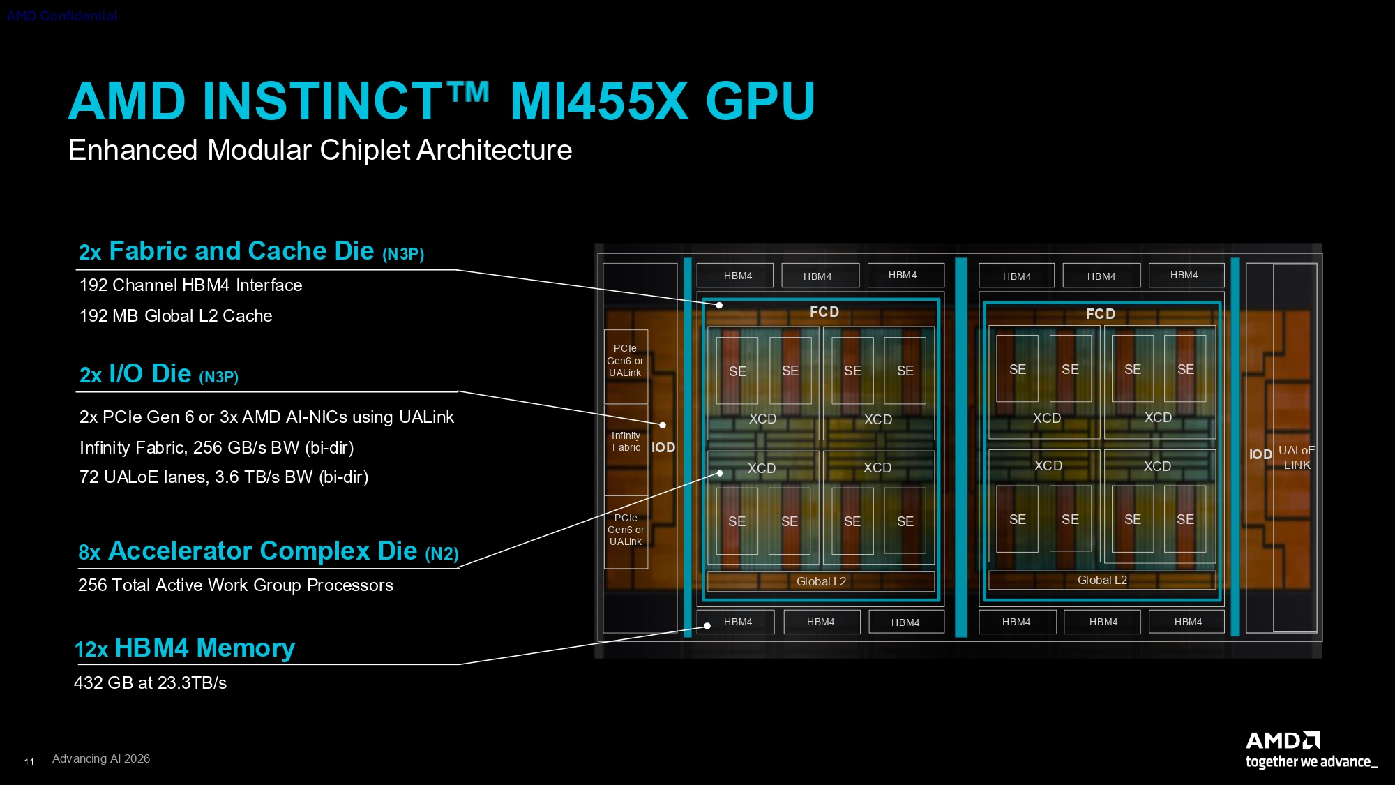
The MI455X is AMD’s forthcoming CDNA 5 AI accelerator for data center training and inference. AMD says the full device contains 320 billion transistors and uses advanced packaging to combine compute, cache, I/O, and HBM4 memory in one accelerator package.
The design uses four Accelerator Complex Dies stacked on each Fabric and Cache Die through hybrid bonding. Two Fabric and Cache Dies connect to 12 total HBM4 stacks, two I/O dies, and each other using TSMC’s CoWoS-L packaging, according to AMD.
AMD is splitting manufacturing where it thinks the density pays off. The compute dies use TSMC’s 2N gate-all-around process, while the Fabric and Cache Dies and I/O dies use TSMC N3P, AMD said. That is the usual chiplet bargain: spend the expensive process where performance and power benefit most, and stop pretending every block deserves the fanciest silicon.
How CDNA 5 changes the GPU
CDNA 5 changes AMD’s programming model in a way developers will actually notice. AMD now refers to the core building block as a Work Group Processor rather than a Compute Unit, and the MI455X keeps the same 256 WGP count as the MI355X. The claimed performance gain therefore has to come from higher throughput per block, not from adding more of them.
AMD also cut the wavefront width from 64 to 32. A wavefront is the group of work items a work group processor handles together. AMD says the smaller width reduces instruction latency, branch divergence penalties, and register pressure, while making it easier to map tensor tile sizes and kernels onto the hardware. AMD’s RDNA graphics chips have used a native 32-wide wavefront since their introduction.
For peak math throughput, AMD says CDNA 5 doubles some rates and quadruples others versus CDNA 4. The company lists the MI455X at 40.26 petaflops for OCP MXFP4, 20.13 petaflops for OCP MXFP6 and MXFP8, 5.03 petaflops for matrix FP16/BF16, and 315 teraflops for vector FP16, matrix FP32, and vector FP32. The same figures in AMD’s comparison put Nvidia Rubin at 35 petaflops for dense NVFP4, 17.5 petaflops for MXFP6 and MXFP8, 4 petaflops for matrix FP16/BF16, 400 teraflops for matrix FP32, and 130 teraflops for vector FP32.
Those comparisons need a warning label. AMD itself acknowledged that real application performance is likely to fall well below peak FLOPS, and software optimization will decide how much of the theoretical hardware shows up in production systems.
Why Helios and HBM4 matter
The MI455X moves to 12 stacks of HBM4, delivering 432GB of memory and 23.3TB/s of bandwidth per GPU, according to AMD. Nvidia’s first Rubin configuration, as described in the same comparison, has 288GB of HBM4 and up to 22TB/s of bandwidth.
Across a 72-GPU Helios rack, AMD says that adds up to 31.1TB of HBM in one coherent GPU domain. The comparable Vera Rubin aggregate cited by AMD is 20.7TB. For inference, where model weights and KV caches punish trips across slower memory paths, that capacity claim is one of AMD’s more concrete shots at Nvidia.
AMD also replaced CDNA 4’s large Infinity Cache approach with a smaller shared L2 cache on each Fabric and Cache Die. Each die carries 96MB of L2, for 192MB total, and AMD says aggregate L2 bandwidth is three times higher than on MI355X. Inside each WGP, local data store capacity doubles to 320KB, with 96MB across the full chip.
Data movement gets its own hardware help. AMD says the CDNA 5 Tensor Data Mover can move data directly from DRAM to the WGP local data store without staging through intermediate cache levels. The company also added multicast memory reads so one read can feed multiple WGPs, reducing duplicated traffic when AI kernels reuse the same weights or activations.
AMD also said it has announced deals with Microsoft and Anthropic tied to this AI push. The harder test comes when MI455X and Helios systems leave slide decks and meet production models, messy kernels, and customers who count tokens per watt.
This story draws on original reporting from Tom's Hardware.