The Sandisk SK hynix HBF spec is now public in outline: the two memory makers have introduced initial specifications for High Bandwidth Flash, a NAND-based memory tier intended to sit beside an AI accelerator. The stated ceiling is 512GB per package, using eight- or 16-die stacks, with three read-bandwidth grades spanning roughly 0.4TB/s to 3.0TB/s. That is a proposed standard, not a GPU product announcement.
Sandisk and SK hynix began an HBF standardization workstream under the Open Compute Project in February. Tom's Hardware reports that the initial specification was released through OCP as an open standard, although the detailed specifications had not yet been officially published by OCP. The document reportedly covers electrical and interface requirements, packaging, reliability guidance and software I/O requirements for stacked HBF devices.
What is HBF and how would it add terabytes of GPU memory?
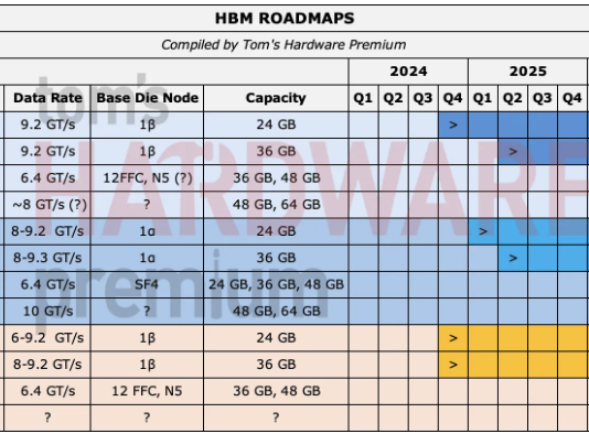
HBF uses specialized NAND flash dies with a fast interface, rather than the DRAM dies used in high-bandwidth memory, or HBM. It is meant to be an additional layer between HBM and SSD storage: closer to compute and far faster than an SSD, but with different compromises from DRAM.
The terabyte claim needs a unit check. The specification's 512GB figure applies to one HBF package. An accelerator would need several HBF packages to reach multiple terabytes. The Register reported that Sandisk materials proposed one design with two HBM stacks and six HBF stacks for 3.12TB of total memory. That is a vendor-proposed configuration, not a shipping accelerator design.
SK hynix describes HBM as the layer for the most demanding bandwidth work, while HBF is intended to expand capacity and improve power efficiency for inference. The practical split is data access: HBM would retain latency-sensitive, frequently updated work, while HBF is pitched for read-heavy data such as pretrained model weights. Those weights are repeatedly fetched as a model produces tokens, a process explained in how LLMs generate answers.
That division exists because NAND does not become DRAM by acquiring a more dramatic acronym. The Register reports that NAND has finite write endurance and microsecond-scale access latency, compared with DRAM latencies measured in tens of nanoseconds. Those traits make HBF a poor fit for the write-intensive and latency-critical parts of inference, and help explain why the companies are presenting it as an HBM complement rather than a replacement.
Does the 3TB/s HBF figure apply to one package?
Available reporting does not settle that. Tom's Hardware says the specification lists bandwidth classes from about 0.4TB/s to 3.0TB/s, but says it is unclear whether the top number describes an individual package or a broader HBF subsystem. Sandisk's reported first-generation target is lower, at up to 1.6TB/s of read bandwidth for a 16-die, 512GB stack. That remains a company target rather than a measured shipping product.
Interface details are also still fuzzy. SK hynix says HBF uses Universal Chiplet Interconnect Express, or UCIe, to connect with heterogeneous computing platforms. Sandisk refers instead to an xPU-HBF interface. Tom's Hardware says the relationship between those descriptions is not yet clear.
Sandisk and SK hynix announced their HBF collaboration in August 2025, then the OCP workstream in February 2026. Broad adoption has not followed from the specification alone: Tom's Hardware reported publicly expressed consortium interest from Google and Tenstorrent, without established commitments from major accelerator suppliers. The available reporting also does not establish an upgrade path for existing consumer GPUs.
This story draws on original reporting from Tom's Hardware.