A Terafab size comparison based on reported square-foot figures puts Elon Musk’s proposed Texas chip factory at roughly four times the combined area of Giga Texas, the Pentagon, Apple Park and the Mall of America. Tesla and SpaceX have confirmed plans for the jointly built semiconductor facility in Grimes County, outside Houston, with a stated first-phase investment of $16.8 billion, according to the New York Post.
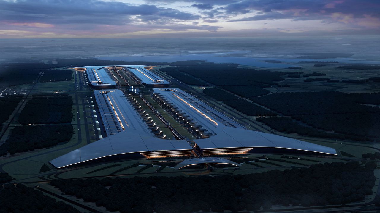
The important qualifier is doing a lot of work here: Terafab is a proposal, not a finished building. Reports describe the completed complex as slated for at least, or more than, 100 million square feet. Whether it takes any world-size record depends on the project being completed at that scale, as pitched.
How big is Terafab compared with the Pentagon and Giga Texas?
Tom’s Hardware reports 10 million square feet for Giga Texas, 6.6 million for the Pentagon, 2.82 million for Apple Park and 5.6 million for the Mall of America. Added together, those figures equal 25.02 million square feet. Dividing Terafab’s 100 million-square-foot projection by that total yields about 4.0.
So the claim that Terafab would exceed all four sites combined is supported by the reported numbers. It would not edge past them. It would be close to four times their stated combined area.
A scale illustration posted by X user Nic Cruz Patane visualizes the comparison, Tom’s Hardware reported. It is an informal graphic, not an engineering drawing or a company site plan, and readers should treat it accordingly.
There is another snag in the viral-building arithmetic. The available accounts use “floor space,” “interior space” and “footprint” for different buildings. Those are not interchangeable measurements: floor area can include multiple levels, while a footprint refers to the ground area occupied by a structure. The comparison is therefore a rough reported-area check, not a precise map of land use or building envelopes.
What would Terafab make?
Tesla and SpaceX say the facility is intended to combine logic-chip and memory production with lithography, packaging and testing under one roof. Semiconductor fabrication is the cleanroom process that builds circuits layer by layer on wafers; packaging and testing are later steps that prepare chips for use and check whether they work.
The companies have framed the factory as a response to their own expected demand for AI compute. Musk has said Tesla and SpaceX will need at least one terawatt of compute, while Tesla has said their future needs would surpass current and expected global chip output, according to the reports. Those are company forecasts, not independently verified production plans.
Musk began discussing an in-house chip plant in late 2025, and the project was formally announced in March, Tom’s Hardware reported. The same report put potential investment across all phases as high as $119 billion and noted that SpaceX has acknowledged the project may not succeed. Nvidia chief executive Jensen Huang has called an undertaking of this sort an “extremely hard” challenge, according to Tom’s Hardware.
The planned site is near Gibbons Creek Reservoir. The New York Post reported that SpaceX said it intends to use reservoir water rather than local groundwater. That addresses one input to a semiconductor plant, but it does not settle the more basic question: whether Tesla and SpaceX can build the integrated operation at the extraordinary scale they are advertising.
This story draws on original reporting from Tom's Hardware.